
Radiation Hardness of CMOS Image Sensor Design

ISDI radiation hard image sensors
ISDI has undertaken image sensor and readout application specific integrated circuit (ROIC) design in several challenging fields including X-ray, proton and electron imaging. These fields share a common challenge – mitigating the damage caused to CMOS image sensors and ROICs by ionising radiation. Designing radiation-hard imaging devices such as X-ray detectors for 24/7 inline operation in electric vehicle battery factories, is one of ISDI’s core capabilities. This blog post explores some of the challenges faced by engineers when designing devices that can operate successfully despite being exposed to high levels of radiation.
In certain applications, such as space missions, satellites, instrumentation for nuclear power plants, experiments with synchrotron light, X-rays, or particle physics, the amount of radiation affecting electronic circuits can be particularly high. In these cases, it is essential to take the necessary precautions to ensure the system's immunity to this factor. Let’s consider the effects of radiation, particularly on silicon, and the methods that allow the system to function even in harsh environments. For an in-depth discussion of the issue, see [1].
Radiation interacts differently with materials depending on the type of incident particle, its kinetic energy, mass, and charge, as well as the mass, atomic number, and density of the material itself.
There are numerous types of particles that may be encountered (photons, neutrons, electrons, protons, and ions being the most common), and the energy levels they can reach vary widely, from a few eV to tens of MeV. However, it is possible to summarize the effects induced in materials into two categories: ionization and damage to the crystalline structure. Heavy particles such as neutrons primarily cause atomic displacement in the crystalline structure, moving atoms to interstitial positions, while photons and electrons typically lead to ionization processes. In some cases, both effects may occur simultaneously, with varying proportions depending on the situation.
In the ionization process, electron-hole pairs are formed in a semiconductor or an insulator in a quantity proportional to the amount of energy absorbed by the material, according to formula (1).
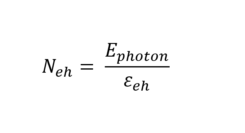
(1)
Where εeh=3.55eV in silicon.
In a MOS structure, on which MOS transistors are based, the carrier pairs generated in the substrate and in the metal or polysilicon gate are quickly removed in the direction of the electric field through the low-resistivity material. In contrast, in silicon oxide, which is an insulator, electrons and holes behave differently, as their mobility ratio varies from 105 to 1012, with an advantage for electrons. Some of the generated pairs (it’s worth mentioning that εSiO2 = 18eV) recombine immediately after generation, while the remaining ones separate according to the present electric field. Assuming a positive voltage is applied to the gate, the faster-moving electrons rapidly migrate towards it (within picoseconds). The holes, on the other hand, move in the opposite direction towards the silicon/oxide interface through a much slower transport phenomenon. Near the interface, still within the oxide, they may be trapped in defects, creating a non-mobile positive charge. Ionization also increases the density of interface traps at the Si-SiO2 boundary by several orders of magnitude, though a definitive explanation of this phenomenon has not yet been formulated.
Damage to the crystal structure, however, is almost negligible in MOS structures because displaced atoms leave behind vacancies (the atom-vacancy pair is known as a Frenkel defect). In silicon oxide at room temperature, for example, 90% of these defects return to their original positions within a minute of radiation exposure ending. In the substrate, the effects are also minimal because conduction occurs through majority carriers (electrons in n-type silicon and holes in p-type silicon), whose behaviour is less influenced by crystal imperfections. This is in contrast to devices that rely on minority carrier conduction, where a locally damaged structure (or even the presence of impurities) reduces the carrier lifetime.
The trapped positive charge in the oxide is positioned at the Si-SiO2 interface when the gate voltage is positive relative to the channel, as occurs in n-channel MOS transistors under normal operation. Conversely, it moves near the SiO2-gate interface when the gate has a lower potential than the channel, typically in p-type MOS devices. The amount of trapped charge depends on the number of defects in the silicon oxide. For this reason, one of the fundamental parameters in designing radiation-immune circuits is the quality of the oxide.
The presence of practically immobile holes in the oxide results in a shift of the MOS structure’s flat-band voltage and, consequently, the transistor’s threshold voltage, which can be calculated as in (2) from [2, p. 460]:
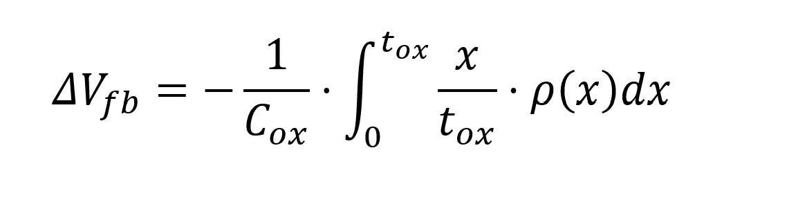
(2)
where Cox is the oxide capacitance per unit area, and ρ(x) is the charge density as a function of the distance x from the oxide-gate interface. It is important to note that the direction of the flat-band voltage shift is always negative when the charge is positive, which is the typical condition. This also means that the gate voltage required to achieve the same inversion conditions in the channel of an n-MOS device is lower in the presence of holes in the oxide, whereas the opposite is true for p-type devices. At high radiation doses, n-MOS transistors may exhibit a threshold voltage too low to be turned off by the driving circuits, or they may even have a zero-threshold voltage, remaining on with VGS=0. A similar effect occurs in p-MOS transistors, but they experience an increase in absolute threshold voltage and have a wider variation margin before their switching becomes impossible.
From equation (2), it is also evident that, for the same total trapped charge, the effects are greater if the charge is located near x = tox, i.e., on the oxide side closest to the channel.
From a circuit design perspective, the effects that must be considered are numerous and sometimes detrimental to system functionality. Leakage current, defined as the current flowing in a MOS device at VGS=0, increases in n-channel devices exposed to radiation, whereas it decreases in p-MOS transistors. Two factors degrade n-MOS performance: first, the subthreshold current increases, particularly due to the reduction in threshold voltage; second, parasitic currents increase due to charge accumulation in the regions adjacent to the gate (Figure 2.9(a)). In the LOCOS (Local Oxidation of Silicon) process, and similarly in STI (Shallow Trench Isolation) for deep submicron technologies, charge accumulation occurs within the field oxide, which is relatively thick and effective in blocking incident particles that generate electron-hole pairs. The trapped charge, which is positively charged for the reasons already described, can create parasitic MOS structures where inversion conditions in the substrate are not externally controllable, leading to significant leakage currents.
The two regions, referred to as the bird’s beak (figure 2.9 (b)), located at the sides of the gate region between the polysilicon and the substrate, are particularly effective in creating alternative current paths between the source and drain. However, inversion can even occur directly beneath the field oxide at high levels of irradiation.
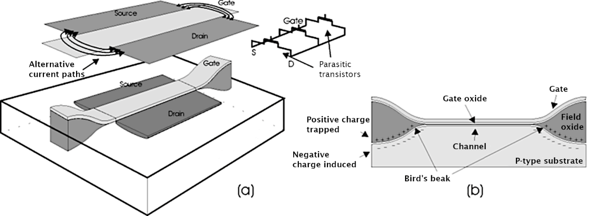
Figure 1: parasitic current paths can form due to accumulation of charge on the edges of the gate (a) and deeper at the bottom of the field oxide (b)
If incident particles are highly energetic (especially heavy ions), they may cause the malfunction of one or more transistors, affecting the reliability of the entire circuit. The resulting error can be reversible (also called a soft error) or irreversible, as in the case of a destructive event (also known as a hard error). A soft error occurs when a particle generates charge along its path in silicon, which is then collected at sensitive circuit nodes. Memory circuits, particularly SRAM (Static Random Access Memory) cells, are highly susceptible to soft errors since their sensitive node is located at the transistor drains. To a greater degree, all sections containing dynamic logic are at risk, as they store a logic level by accumulating or removing charge at an internal node. These anomalies can lead to erroneous signals in analogue circuits or temporary issues in digital components (such as sequential logic lock-ups or execution errors in programmes), but they can be resolved by applying a reset signal or reloading the programme into memory.
Hard errors are more serious, as they prevent the system from returning to operational conditions without replacing damaged components. One example is latch-up in CMOS structures, which can be caused by high substrate currents, elevated temperatures, or charge generation at parasitic transistor bases [3]. In such cases, only a rapid shutdown of the circuit can prevent permanent damage to the die.
The advancement of technology has significantly increased circuits’ intrinsic resistance to radiation by using ultra-thin gate oxides (on the order of ten nanometres or less in 0.25μm processes), which are easily penetrated by particles, leading to minimal material interactions and fewer generated electron-hole pairs. Measurements show that for oxide thicknesses up to ~20nm, the flat-band voltage shift (and thus threshold voltage variation) decreases proportionally to tox² with a further reduction below this thickness.
The measured data found in the literature have shown, for example, a ∆Vth of 300mV/Mrad at tox=20nm in 0.8μm technology, ∆Vth of 80mV/Mrad at tox=10nm for 0.5μm technology, and finally ∆Vth of 5mV/Mrad at tox=6nm in 0.25μm technology [4]. It should be noted that the transistor threshold scales much less aggressively between technologies, so the robustness is improved with technology downscaling. It is therefore possible to use submicron commercial CMOS technologies even in environments with high radiation levels, such as particle detectors in accelerators or radiographic and diffraction imaging.
Regarding destructive events such as latch-up, modern technologies once again offer a reliable solution. Specific design measures have been implemented to reduce the likelihood of triggering parasitic bipolar transistors within CMOS structures, including epitaxial substrate growth, retrograde wells, and trench isolation. The epitaxial layer has been introduced to achieve lower substrate resistance without altering the doping level in the channel region. The approach involves growing a thin epitaxial layer of a few microns thickness on a highly doped (low-resistivity) silicon substrate with a lower dopant concentration. Retrograde wells also aim to reduce semiconductor resistance by employing a special doping profile that increases dopant concentration at the bottom of the well. Finally, trench isolation separates adjacent transistors using deep trenches filled with oxide, significantly reducing the gain of lateral parasitic bipolar transistors while also allowing for a smaller minimum spacing between devices.
In some respects, the reduction in feature size in modern processes does not always have beneficial effects. Considering soft errors caused by charge deposition at critical circuit nodes, smaller devices inherently store less charge on parasitic capacitances, making them more susceptible to lower-energy particle strikes that could corrupt memory contents. As for oxide breakdown, while it is currently unlikely at present thicknesses, further reduction combined with increased maximum electric field values could become problematic.
Several layout techniques have been explored to make commercially available deep submicron technologies suitable for use in radiation-exposed environments. The key issue is reducing leakage currents in n-type devices due to the accumulation of positive charge in the field oxide (Figure 2.10(a)). Various solutions exist: one approach is to extend the length of parasitic structures (Figure 2.10(b)) by designing longer gates at the edges of the channel while maintaining nominal length at the center, though this method may be ineffective. Alternatively, the field oxide region can be moved away from the channel by introducing a p+ diffusion (known as a guard ring) around the transistor, ensuring only thin oxide within its boundary (Figure 2.10(c)). This method preserves the original device dimensions but is often restricted by layout design rules; additionally, its radiation resistance is limited since an alternative leakage path can still form at high radiation doses. The most robust solution is an Enclosed Layout Transistor (ELT), which completely eliminates the parasitic device and thus the risk of leakage currents. This structure features a circular gate with drain and source located inside and outside the gate, respectively (Figure 2.10(d)). However, drawbacks include increased area consumption, difficulty in determining the W/L ratio for simulations, and the inability to implement arbitrary W/L ratios available in standard devices. Additionally, ELTs exhibit higher parasitic drain and source capacitances and structural asymmetry.
Surrounding the device with a grounded p+ diffusion remains effective in preventing unintended current paths between n+ diffusions of adjacent transistors, albeit at the cost of reduced achievable device density.
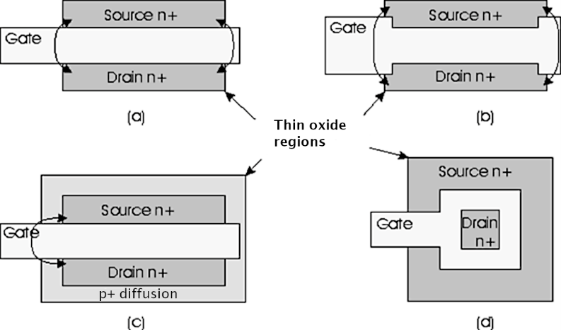
Figure 2: Layout techniques to reduce leakage current shown in (a): lengthening the gate of parasitic devices (b), increasing the distance between the field oxide region and the gate (c), and using ELT design (d).
Careful physical implementation at the silicon level can enhance resistance to destructive events. Several recommendations exist to minimize the likelihood of latch-up:
Using numerous well and substrate contacts.
Increasing the spacing between p+ diffusions in n-wells and n+ diffusions in p-type substrates.
Introducing n+ diffusions around p-MOS transistors, in addition to the p+ diffusions around n-MOS transistors already mentioned for leakage current mitigation. This measure reduces the gain of the parasitic PNP transistor (or NPN for n-MOS) by introducing a conductive region in the base connected to the supply voltage.
It is important to note that guard rings cannot be crossed by polysilicon interconnections, as they are created using the same process steps used for drain and source diffusions. Consequently, they would be interrupted under the polysilicon, effectively forming an unintended transistor. This also contributes to increasing the area required by the structure.
0.25μm technologies have demonstrated particularly high resistance to latch-up [5], even without guard ring diffusions around active devices. Therefore, in conditions where total absorbed dose is not extreme, their use is sufficient to ensure radiation tolerance.
[1] G. M. Anelli, “Design and characterization of radiation tolerant integrated circuits in deep submicron CMOS technologies for the LHC experiments”, These pour obtenir le grade de DOCTEUR DE L’INGP, Institut National Polytechnique de Grenoble, 11 december 2000
[2] R. S. Muller, T. I. Kamins, “Device Electronics for Integrated Circuits”, Wiley, 1886
[3] J. M Rabaey, “Digital Integrated Circuits – a design perspective”, Prentice Hall, 2000 pp.56, 57
[4] J. V. Osborn, R. C. Lacoe, D. C. Mayer and G. Yabiku, “Total Dose Hardness of Three Commercial CMOS Microelectronics Foundries”, IEEE Transactions on Nuclear Science, Vol. 45, no. 3, June 1998, pp. 1458-1463.
[5] C. Brothers, R. Pugh, P. Duggan et al., “Total-Dose and SEU Characterization of .25 Micron CMOS/SOI Integrated Circuit Memory Technologies”, IEEE Transactions on Nuclear Science, Vol. 44, no. 6, December 1997, pp. 2134-2139.