
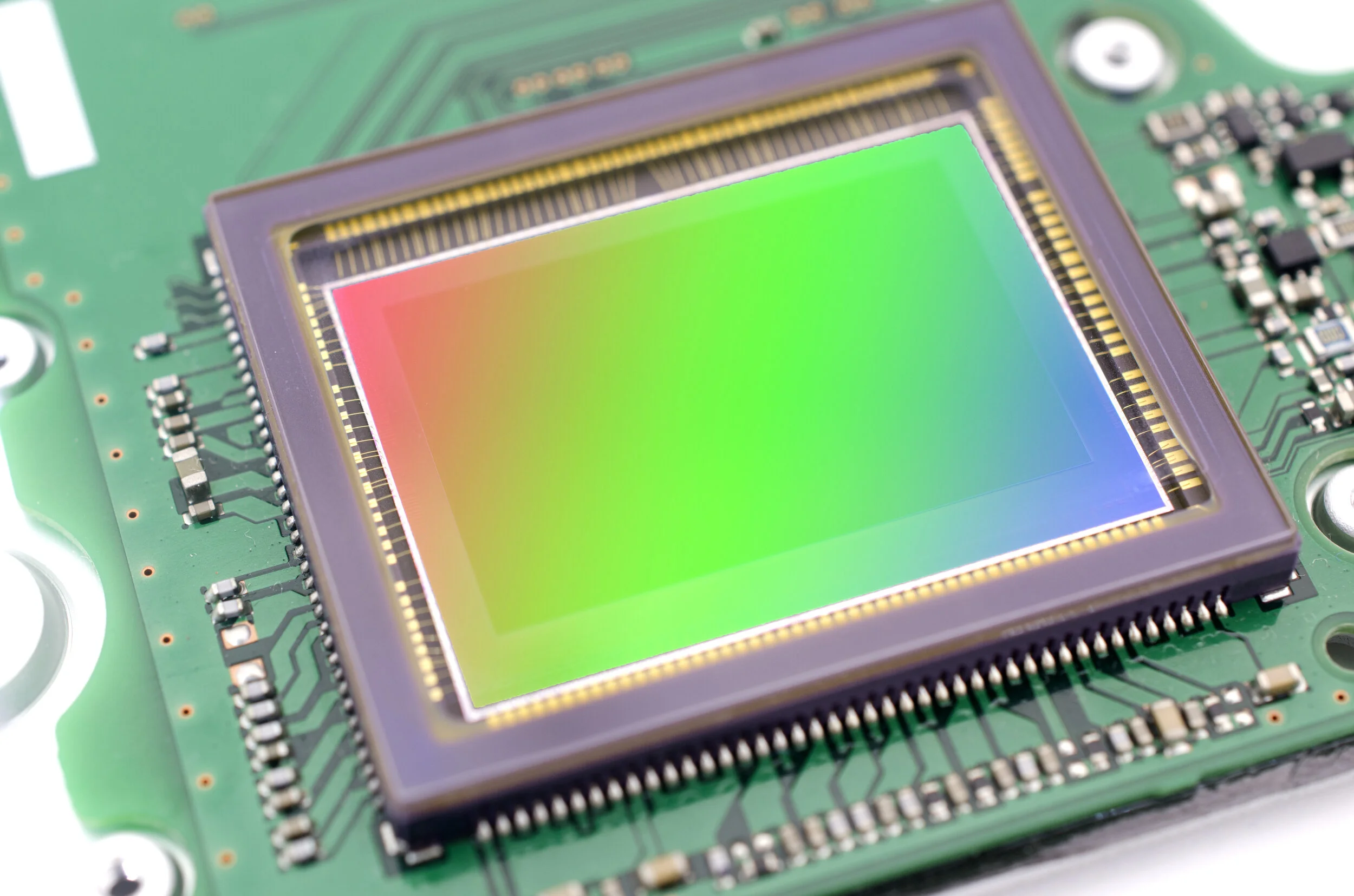
ACTIVE PIXEL SENSORS
The CMOS active pixel sensor (APS), first developed in the 1990s, has progressively replaced other forms of solid state imaging technology such as the charge-coupled device (CCD) and thin film transistor (TFT). While these technologies are still used for certain applications, CMOS is now the mainstream technology in most imaging device today, ranging from low-cost mobile phone cameras to advanced 3D sub-atomic particle detection systems.
The reasons behind the explosion of CMOS imaging devices are cost and performance. CMOS devices can be mass produced with low cost, while the advance of chip technology has ensured that CMOS performance can excel in terms of low noise, stability and high speed.
The original APS was built around a simple circuit topology of a photodiode and 3 or 4 transistors. As Moore’s Law enabled ever greater complexity in a smaller scale, pixels can now have complexity, and can incorporate photon counting and digital logic.
ISDI’s patented pixel design combines advanced low noise design with radiation-hard properties, making it ideal for X-ray applications.
Our wide experience in research projects and non-standard sensor design provides capabilities to design for a wider spectral sensitivity, ranging from near infrared to ultraviolet. Our knowledge of scintillators and conversion techniques allows us to design X-ray detectors with photon detection from low kV to MV.
ISDI Technology portfolio includes:
Photon counting
Linear arrays
Image Sensors
1D/2D stitching
Silicon Strip Sensors
CdTe – CdZnTe
Single Ramp 8-16bit
Cyclic up to 12-18bit
Radiation tolerance
Radiation hardness of CMOS Image Sensor Design
Data interfaces
LVCMOS
LVDS
Programming interfaces
SPI
Custom
I2C
Auxiliary blocks
Analogue: Bandgaps/current refs/temp sensors/local oscillators/PLLS/DC-DC
Digital: data Serializers/ADC ECL/programmable ROW decoders/FSM for sequencing
Smart sensors
Sensors for rad hard environments
