CMOS Stitching Design
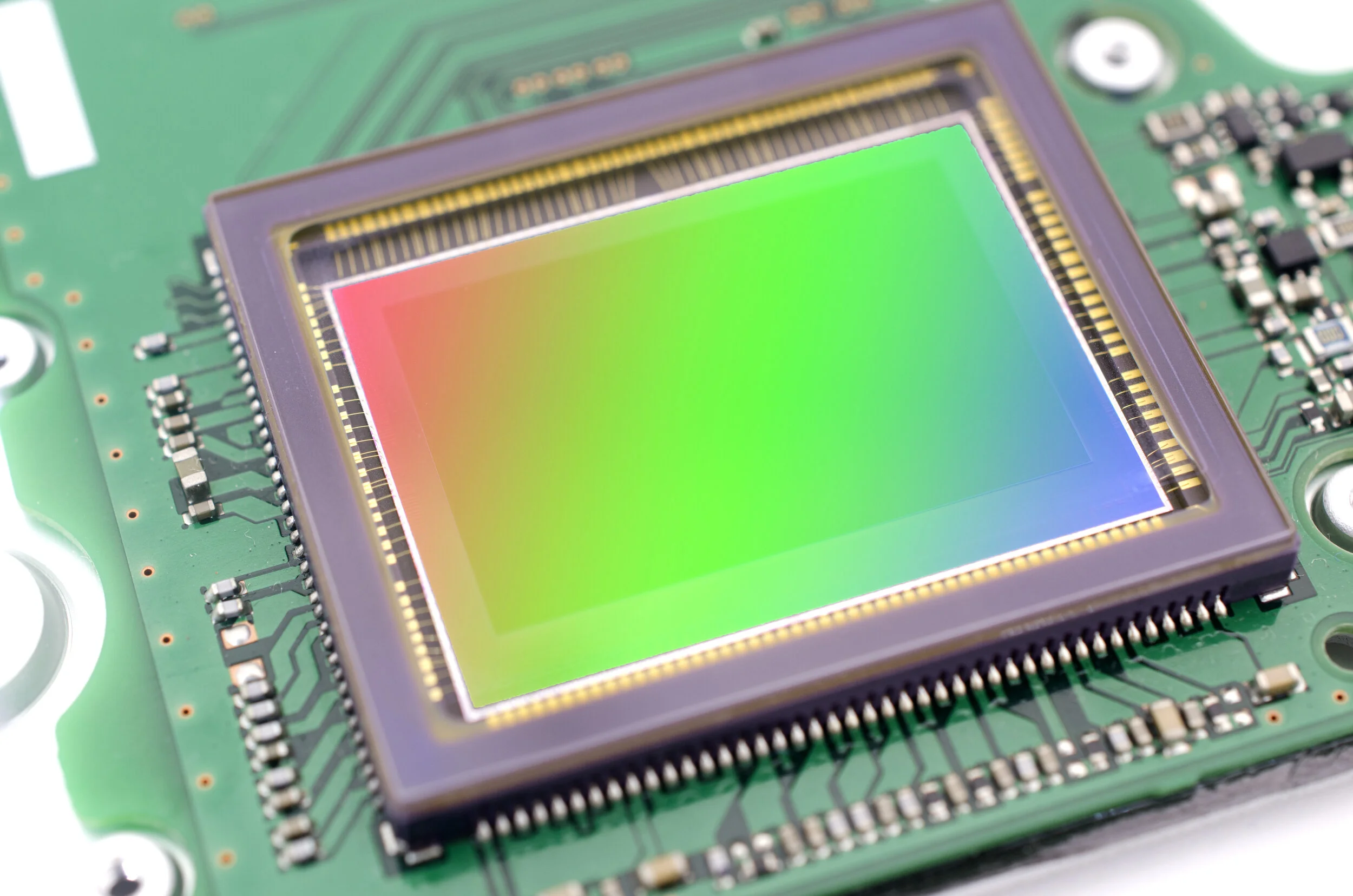
ISDI offers advanced CMOS stitching design services, a specialized technique in semiconductor manufacturing for constructing large CMOS sensors and ASICs. By meticulously “stitching” together smaller sections, or sub-reticles, of a chip design, we enable the creation of expansive sensors crucial for applications in medical imaging, industrial cameras, and large-format scanning.
Precision Integration for Seamless Results:
CMOS stitching requires an exceptionally high level of precision to seamlessly integrate multiple sub-reticles. Our Project Managers and Integrated Circuit Layout Design Engineers are highly skilled in addressing the specific challenges of CMOS stitching. They apply innovative layout techniques, ensuring electrical continuity and circuit performance even when dealing with large-area silicon designs.
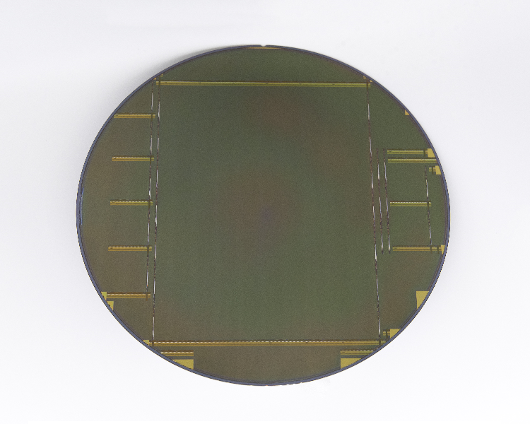
The stitching blocks drawn on one of the many lithographic masks used for the production of the image sensor
Key Service Features:
Lithographic Mask Design & Stitching Regions: We develop stitching blocks on photolithographic masks that are precisely aligned for optimal sensor performance. The designated “stitching regions” on the edges of each sub-reticle are carefully managed to prevent open connections, short circuits, and design rule violations.
Signal Routing and Modular Design: Our approach to signal routing tackles the large parasitic capacitance and resistance in extended layouts, enhancing performance consistency. Modular design strategies also allow for hierarchical verification across thousands of ADCs and millions of pixels.
Advanced Verification Techniques: We conduct thorough Design Rule Checks (DRC), Layout Versus Schematic (LVS) analysis, and Repeated Patterns Checks to ensure layout consistency across all reticle rows. This minimizes potential yield losses associated with stitching, ensuring the highest quality in production.
Managing Challenges in CMOS Stitching:
Achieving a flawless CMOS stitch is no small feat. Our team applies years of expertise to handle the inherent complexities of stitching, from seamless alignment to managing intricate design rules and dealing with large-area silicon yields. Through rigorous testing and verification, we ensure that each stitched sensor meets ISDI’s high standards.
Why Choose ISDI for CMOS Stitching?
When creating large CMOS sensors and ASICs, ISDI Sensors R&D Austria delivers results that meet the highest technical standards in the industry. Our comprehensive service—from initial layout design to final verification—ensures that CMOS stitching is a “seamless” process, setting the foundation for optimal functionality and reliability in even the most demanding applications.
Contact us today to learn more about our CMOS stitching services and how we can support your high-performance sensor and ASIC manufacturing needs.
A CMOS wafer containing a single stitched image sensor


